Study of excitonic and spin-valley properties
in transition metal dichalcogenide (TMDC) monolayers
CONTEXT.
Layered materials are known for centuries. Nevertheless, the potential of these materials has been re-considered during the past decade thanks to the investigation of individual layers obtained by mechanical or chemical exfoliation. When thinned down to one monolayer, these materials can exhibit completely different properties from their bulk counterparts. Atomically thin carbon layers (graphene) have been the first 2D material to stimulate intense research due to its high carrier mobility and thermal conductivity. But recently, many other layered materials have been thinned down to the monolayer limit leading to a wide range of new promising 2D semiconductors, insulators, metals and even superconductors.
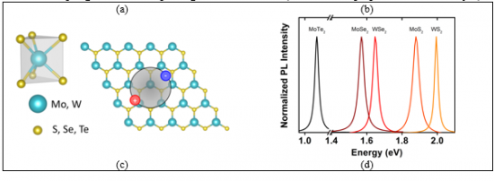
Among the various families of 2D materials, 2H semiconducting transition metal dichalcogenide (TMDC) materials MX2 (where M stands for Mo or W and X stands for S, Se or Te) exhibit especially exciting properties when thinned down to one monolayer. (Fig. 1).
Among the various families of 2D materials, 2H semiconducting transition metal dichalcogenide (TMDC) materials MX2 (where M stands for Mo or W and X stands for S, Se or Te) exhibit especially exciting properties when thinned down to one monolayer. (Fig. 1).
i. Despite being indirect band gap semiconductors in their bulk form, TMDC materials become direct band gap when thinned down to one ML1,2. The direct band gap is located at the K points of the hexagonal Brillouin zone and ranges from 1 eV (MoTe2) to 2 eV (WS2) (Fig. 1(b)) making TMDC MLs particularly attractive materials for electronics and optoelectronics applications with visible to near infrared wavelengths.
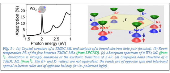
ii. In TMDC MLs, electron-hole pairs are strongly bound by the Coulomb interaction to form robust excitons with binding energies of several hundreds of meV. Consequently, a strong light-matter interaction occurs with optical properties mainly governed by excitonic states even at room temperature. For example, when resonant with excitonic states, light absorption/ML can reach 15%3,4 (Fig. 1(c)) while non-linear effects5 and coupling to phonons6,7 are enhanced by several orders of magnitude. Because of the very large exciton binding energy TMDC MLs are also attractive systems to study strong coupling exciton-polariton physics at room temperature.
iii. Due to the lack of crystal inversion symmetry, the optical selection rules in K+ and K- valleys depend on the helicity of light8 (left circularly polarized σ+ in K+ valleys and right circularly polarized σ- in K- valleys) (Fig. 1(d)). This gives an optical access to a new degree of freedom (the valley index, sometimes called valley pseudospin) that can be used for data processing or storage. In addition, TMDC materials are characterized by a large spin-orbit coupling (SOC) which is expected to stabilize the valley pseudospin by coupling it to the true spin degree of freedom SZ (z direction is perpendicular to the layer).
OPTICAL SPECTROSCOPY ON 2D MATERIALS AT THE LPCNO TOULOUSE.
Our group is using several low vibration, closed cycle cryostats at the heart of our optical spectroscopy set-ups. We can perform photoluminescence and absorption measurements at variable temperature (4K to room temperature) with a spatial resolution of the order of 1 micro meter with detailed polarization analysis. For time integrated detection we use back illumination, deep depletion silicon CCDs and InGaAs based detectors. For time resolved experiments we use streak camera detection systems with resolutions in the ps range. We can apply magnetic fields in magneto cryostats in 1 dimension (9 Tesla) and 3 dimensions (Vector magnet : 5T – 2T – 2T). For excitation we use pulsed and continuous wave tunable sources (Ti-Sa lasers, frequency doubler, OPO).
SAMPLE FABRICATION AT THE LPCNO.
We use mechanical exfoliation techniques (scotch tape technique) to isolate monolayers and deterministic transfer (PDMS stamping) to fabricate van der Waals heterostructures (stacking of 2D layers). For example we can encapsulate 2D semiconductors between hexagonal Boron nitride (hBN) layers to reduce inhomogeneous effects and use graphene layers as contact electrodes to fabricate charge tunable structures. The high quality TMDC bulk material is sourced in part from the group of Sef Tongay at Arizona State University, the excellent hBN is provided by our collaborators T. Taniguchi and K. Watanabe (NIMS, Japan).
General References
1 K.F. Mak et al., Phys. Rev. Lett. 105, 136805 (2010). 2 A. Splendiani et al., Nano Lett. 10, 1271 (2010). 3 Y. Li et al., Phys. Rev. B 90, 205422 (2014). 4 M. Amani et al., Nano Lett. 16, 2786 (2016). 5 G. Wang et al., Phys. Rev. Lett. 114, 097403 (2015). 6 A.M. Jones et al., Nat. Phys. 12, 323 (2016). 7 G. Wang et al., Phys. Rev. Lett. 115, 117401 (2015). 8 D. Xiao et al., Phys. Rev. Lett. 108, 196802 (2012).
Publication of LPCNO on TMDCs
– Fine Structure and Lifetime of Dark Excitons in Transition Metal Dichalcogenide Monolayers. Physical Review B 96, 155423 (2017)
– Gate controlled spin-valley locking of resident carriers in WSe2 monolayers. Physical Review Letters 119, 137401 (2017)
– Charged excitons in monolayer WSe2: experiment and theory. Physical Review B 96, 085302 (2017)
– In-plane Propagation of Light in Transition Metal Dichalcogenide Monolayers: Optical Selection Rules. Physical Review Letters 119, 047401 (2017)
– Excitonic Linewidth Approaching the Homogeneous Limit in MoS2-Based van der Waals Heterostructures. Physical Review X 7 (2), 021026 (2017)
– Intrinsic exciton-state mixing and nonlinear optical properties in transition metal dichalcogenide monolayers. Physical Review B 95 (3), 035311 (2017)
– Enabling valley selective exciton scattering in monolayer WSe2 through upconversion. Nature Communications 8, 14927 (2017)
– Control of exciton valley coherence in transition metal dichalcogenide monolayers. Physical review letters 117 (18), 187401 (2016)
– Excitonic properties of semiconducting monolayer and bilayer MoTe2. Physical Review B 94 (15), 155425 (2016)
– Ultra-low power threshold for laser induced changes in optical properties of 2D molybdenum dichalcogenides. 2D Materials 3 (4), 045008 (2016)
– Domain architectures and grain boundaries in chemical vapor deposited highly anisotropic ReS2 monolayer films. Nano letters 16 (9), 5888-5894 (2016)
– Well separated trion and neutral excitons on superacid treated MoS2 monolayers. Applied Physics Letters 108 (25), 251106 (2016)
– Exciton radiative lifetime in transition metal dichalcogenide monolayers. Physical Review B 93 (20), 205423 (2016)
– Discrete quantum dot like emitters in monolayer MoSe2: Spatial mapping, magneto-optics, and charge tuning. Applied Physics Letters 108 (14), 142101 (2016)
– Splitting between bright and dark excitons in transition metal dichalcogenide monolayers. Physical Review B 93 (12), 121107 (2016)
– Exciton states in monolayer MoSe2: impact on interband transitions. 2D Materials 2 (4), 045005 (2015)
– Spin and valley dynamics of excitons in transition metal dichalcogenide monolayers. Physica Status Solidi B 252 (11), 2349-2362 (2015)
– Double resonant Raman scattering and valley coherence generation in monolayer WSe2. Physical review letters 115 (11), 117401 (2015)
– 2D materials: ultrafast exciton dynamics. Nature materials 14 (9), 860 (2015)
– Magneto-optics in transition metal diselenide monolayers. 2D Materials 2 (3), 034002 (2014)
– Polarization and time-resolved photoluminescence spectroscopy of excitons in MoSe2 monolayers. Applied Physics Letters 106 (11), 112101 (2015)
– Giant enhancement of the optical second-harmonic emission of WSe 2 monolayers by laser excitation at exciton resonances. Physical review letters 114 (9), 097403 (2015)
– Valleytronics: Divide and polarize. Nature Physics 11 (2), 94 (2015)
– Spin-orbit engineering in transition metal dichalcogenide alloy monolayers. Nature Communications 6, 10110 (2015)
– Exciton dynamics in WSe2 bilayers. Applied Physics Letters 105 (18), 182105 (2014)
– Exciton valley dynamics probed by Kerr rotation in WSe2 monolayers. Physical Review B 90 (16), 161302 (2014)
– Valley dynamics probed through charged and neutral exciton emission in monolayer WSe2. Physical Review B 90 (7), 075413 (2014)
– Exciton fine structure and spin decoherence in monolayers of transition metal dichalcogenides. Physical Review B 89 (20), 201302 (2014)
– Carrier and polarization dynamics in monolayer MoS2. Physical Review Letters 112 (4), 047401 (2014)
– Strain tuning of optical emission energy and polarization in monolayer and bilayer MoS2. Physical Review B 88 (12), 121301 (2013)
– Robust optical emission polarization in MoS2 monolayers through selective valley excitation. Physical Review B 86 (8), 081301 (2012)
Main collaborations
I. Gerber (LPCNO-Physical and Chemical Modelization team): DFT-GW-BSE calculations
M. Glazov, E. Ivchenko (Ioffe Institute Saint Petersburg Russia): modeling of excitonic propertiess
S. Tongay (Arizona State University USA): synthesis of layered materialss
K. Watanabe, T. Taniguchi (NIMS Japan): synthesis of hexagonal boron nitride (hBN)s
S. Crooker (Los Alamos USA): time-resolved Kerr rotation spectroscopys
Funding
ANR JCJC. Vallex (2017-2020)
Labex Next. VW-Spin (2017-2019)
Labex NEXT. METCO (2017-2019)
ANR. MoS2ValleyControl (2014-2017)
Labex Next. Valleyhall (2013-2015)
ERC OptoDNPcontrol (2013-2018)
ITN SpinNANO (2016-2020)
Contacts
cedric.robert@insa-toulouse.fr
bernhard.urbaszek@insa-toulouse.fr