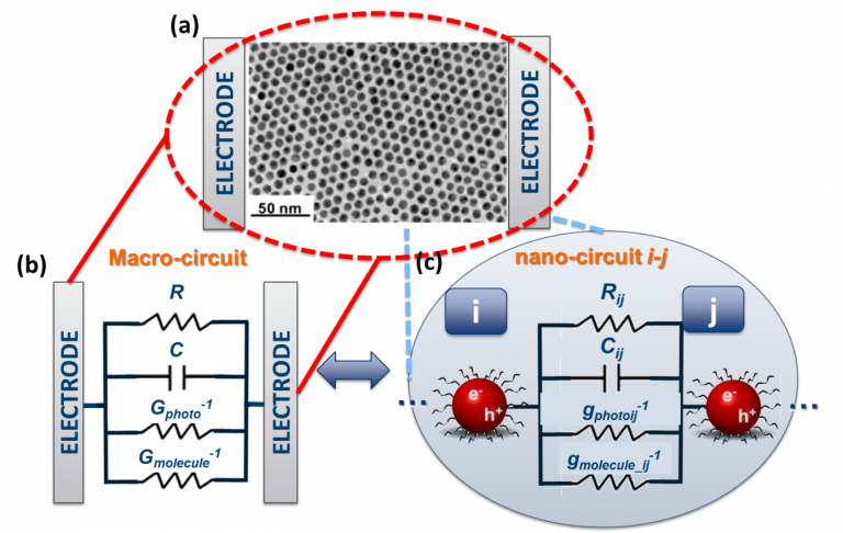
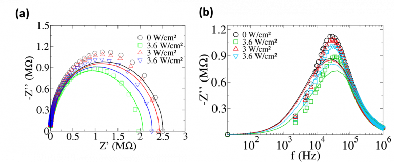
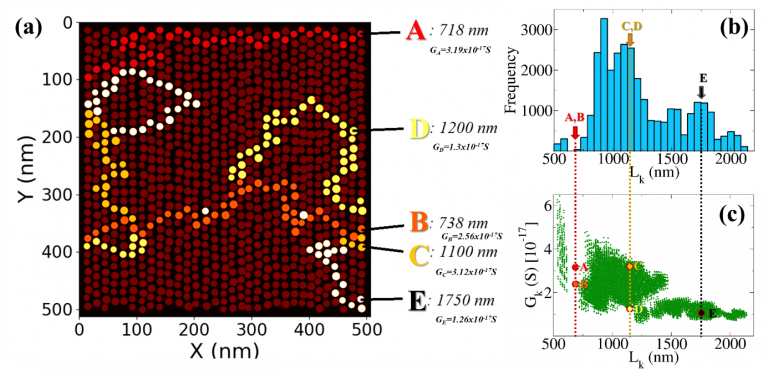
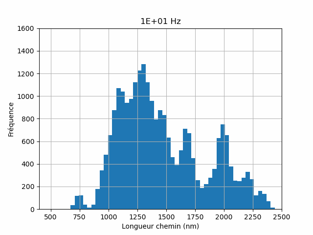
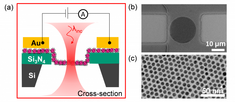
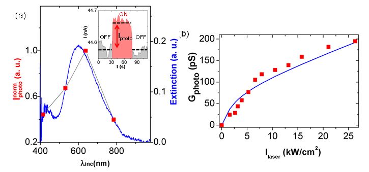
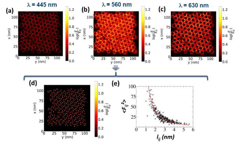
Nanotech

Development of “plasmo-electronics”

In collaboration with Adnen Mlayah (LAAS/CNRS) (adnen.mlayah@laas.fr), we develop the plasmo-electronics field, coupling between plasmonic phenomenon and electron transport of metallic nanoparticles assemblies surrounded by organic ligands.

Plasmonic metal nanostructures have recently attracted extensive research and been exploited for enhancing the performance of various optoelectronic devices (1-5). Colloids composed of metallic nanoparticles (NPs) coated by organic ligands have been used to fabricate hybrid molecular networks contacted by nanoelectrodes (5-8). Overall, coupling localized electron oscillations with charge transport leads to an emerging field called “plasmo-electronics” that could provide a new class of light responsive materials.

The driving force behind the developing “plasmo-electronics” discipline is the link between charge transport and surface plasmons in metal nanostructures. It has been demonstrated that charging metal nanoparticles can change their plasmonic response and that plasmonic excitations of a nanoparticle assembly can affect macroscopic flows of charges (14). Particularly, it has been shown that a rise (positive photo-conductance) or decrease (negative photo-conductance) in conductance upon optical irradiation tuned to the nanoparticles surface plasmon resonance, can occur (15,16). In this situation, it had been found that negatively charged ligands act as charge traps lowering the free carrier density and resulting in a negative photoconductance. However, since positive photo-conductance with charged ligands has also been discovered, this view has been hotly contested in the literature (17-19). 

These phenomenon are quite complex and involve several interaction steps (plasmon-photon, electron-electron, electron-phonon), but it is still poorly understood in terms of the relationship between local opto-electronic properties at the nanoparticle scale and the macroscopic characteristics of the photoconductance (spectral dependence and positive or negative).

In this respect, on one hand, we have experimentally previously demonstrated, using impedance spectroscopy, that both resistive and capacitive characteristics are complementary and can be used to further understanding the charge transport properties of self-assembled nanoparticle networks [Ref]. These studies demonstrated that the entire NP assembly can be modeled as an equivalent electrical macro-circuit made up of a parallel resistance R and capacitance C.

On the other hand, we demonstrated that utilizing numerical simulations in conjunction with light irradiation dependent impedance spectroscopy measurements, it is possible to connect the macro- and nano-scale opto-electronic properties of metal NPs assemblies. The electrical characteristics were modeled using numerical simulations of a collection of interconnected local nano-circuits while accounting for the inter-particle resistance Rij and capacitance Cij. To account for the positive and negative photoconductance generated by the light induced charge generation and transport, a local positive photoconductance gij and a local molecule conductance are added at the nano-circuit level. The approach developed in this project is based on numerical simulations of the dynamical charge transport properties of a network composed of elementary electric nano-circuits (Figure 1).

Figure 1: (a) TEM image of the NP network, (b) microscopic resistance R, capacitance C, Gphoto-1 and Gmolecule-1 of the macro-circuit resulting from the charge transport over the whole network formed by inter-connexion of elementary nano-circuits (c). The latter are formed by inter-particle resistance Rij, capacitance Cij , gphoto_ij-1 and gmolecule_ij-1.

By resolving Kirchhoff’s laws, the current passing through the nanoparticle assembly is determined. This method enables the definition of a macroscopic positive and negative photoconductance that can be obtained using impedance spectroscopy measurements carried out under light illumination. The simulator was used to bridge the gap between nano and macro-scale and finally found a good agreement between simulations and experiment at the macroscale (Figure 2).

Figure 2: Comparison of experimental (symbols) and simulated curves (straight lines) of (a) Nyquist’s impedance plots for dark conditions and laser power of 3.6, 3.6 and 3W/cm² for = 405, 532, 640 nm respectively and (b) imaginary part of the impedance as a function of frequency.

The numerical simulations are thus capable of capturing the essential physics of the coupling between charge transport and plasmonic properties of complex nano-composite materials. The numerical simulations have a capability of reconstructing conduction paths (Figure 3) and can thus address the distribution of path lengths (Figure 4).

Figure 3: (a) Spatial distribution of five selected paths of the histogram of the simulated network at f0 frequency (f0= 1x10⁴ Hz): A = (3.19x10⁻¹⁷S, 718nm), B = (2.56x10⁻¹⁷S, 738 nm), C = (3.12x10⁻¹⁷ S, 1100 nm), D = (1.3x10⁻¹⁷ S, 1200 nm) and E = (1.26x10⁻¹⁷ S, 1750 nm) (b) and (c) are Histograms of conduction path lengths and conductance as a function of path length extracted from the numerical simulations of a hexagonal lattice network formed by gold nanoparticles including 15% size fluctuations at f0.[17]
Figure 4: Animated gif of the evolution of the Pathway histograms as a function of the frequency of the exciter signal.

In this way we are able to assess the efficiency of the light-to-current conversion at the nano-scopic level. Such a physical quantity is very difficult to obtain experimentally including in near-field based optical spectroscopy techniques. The simulator allows to test several physical models at the nano-scale to compare them to the experiments.

In particular, with the type of sample developed below. In order to understand the interplay between surface plasmon resonance and electrical conductance and mechanisms at stake, it is primordial to lower the influence of parasite parameters such as substrate of the assemblies and to provide a model system (Fig. 5). So far, we managed to assemble robust, conductive, monolayered, free-standing NP arrays, so called NP membranes.

Figure 5: a) Schematic cross-section of a contacted freestanding monolayered Au nanoparticle (NP) membrane, under laser beam illumination. b) Scanning electron microscopy image of a freestanding monolayered dodecanethiol coated 7 nm Au NP membrane suspended over a 20 μm wide Si3N4 stencil aperture substrate with two gold microelectrodes as contacts. c) transmission electron microscopy (TEM) image of a freestanding monolayered membrane of 7 nm dodecanethiol coated Au NPs.

The Stencil membranes developed in this project are the result of a long collaboration with Jürgen Brugger (EPFL, https://people.epfl.ch/juergen.brugger?lang=en)

In this work, we investigate the photoconductance generation in NP membranes under focused laser illumination. We carried out that the amplitude of the induced current is correlated with the plasmonic resonance of the NP arrays (Fig. 6a) but also strongly depends of illumination power (Fig. 6b) and polarization voltage.

Figure 6: a) Normalized plasmonic photocurrent I_photo^norm and optical extinction spectrum of a freestanding monolayered membrane as a function of incident wavelength λinc. Inset: Electrical current as a function of time with the laser beam alternating from OFF to ON and back to OFF states (λinc = 638 nm, ILaser = 5.2 kW/cm2, +1V). The OFF and ON states are highlighted by grey and red areas, respectively. b) Plasmon-induced conductance Gphoto (red squares) as a function of illumination ILaser. The blue curve is the best-fitted curve using our model.

The absence of a substrate also leads to a 50% raise of the photocurrent at the resonant wavelength. DDA simulations showed that at least half of this increase is due to the optical properties of the substrate. Finally, accordingly to the temperature dependence of electrical conductance, the photocurrent in the free-standing NP membrane can be interpreted as a combination of a trap state dynamics and a thermally activated phenomenon yielding a temperature rise estimated at 40K at plasmon resonance for Ilaser~5.3kW/cm2. Moreover, intrinsic plasmo-electronic properties have been measured with no influence of a substrate allowing a superior transduction for better sensing or hyperthermia applications. 

From nanoscale to macroscale using DDA-Kirchhoff approach:

How to get the local photo-electric conversion between two neighbouring nanoparticles ?  

A local plasmonic-electronic nanojunction is introduced, as the fundamental building
block of a mesoscale electrical network, and serves as the beginning point for the development of a multiscale modeling strategy. The interparticle charge tunneling and accumulation account for the dynamical charge transport; the plasmoelectronic properties are implemented at the nanoscale using electrodynamic calculations based on the discrete dipole approximation (DDA) method. The electric characteristics of the macroscopic NP network are calculated using a numerical resolution of the current-bias equations based on Kirchhoff’s laws. Disorder effects due to size and position fluctuations of the NPs within the network as well as dislocations and point defects in their spatial arrangement are taken into account. The effects of light excitation intensity and wavelength on the nanojunction photoconductance and on the macroscopic photoresistance of the NP network are addressed. In particular, plasmoelectronic conduction paths are extracted from the coupled DDA-Kirchhoff numerical simulations, and their statistical distribution is investigated as well as their dependence on path length.

Figure 7: Electric field intensity enhancement F_ij (λ)=|E_ij (λ)/E_0 | calculated using DDA simulations performed on a 100 nm x 100 nm nanoparticle assembly shown in Figure ESI 1a. Maps of 〖F_ij〗^2 calculated around the surface plasmon resonance at 445 nm (a), 560 nm (b) and 630 nm (c). The excitation wave is circularly polarized in the assembly plane, (d) Map of the field intensity enhancement calculated at 560 nm and averaged over the gap distance between each pair of nanoparticles; (e) plot of as a function of inter-particle distance lij.

The theoretical results are compared with impedance spectroscopy measurements performed under optical excitation. We found a good agreement between the predicted impedance Nyquist plots and resonance properties, and the measurements. In particular, we were able to estimate the surface plasmon-assisted photoelectric conversion efficiency involving first neighbor NPs. We found that the photoconductance of a single nano-junction formed by a dimer of nearly touching NPs is around 18 nS/W/cm2 [18] under resonant plasmonic excitation. The presented project provides insight into the photoinduced charge transport in self-assembled NP networks and opens the route to novel applications in the field of plasmoelectronics.

REFERENCES:

1  K. R. Catchpole and A. Polman, Appl. Phys. Lett., 2008, 93, 191113.
2  H. A. Atwater and A. Polman, Nat. Mater., 2010, 9, 205–213.
3  J. Liao, S. Blok, S. J. van der Molen, S. Diefenbach, A. W. Holleitner, C. Schönenberger, A. Vladyka and M. Calame, Chem Soc Rev, 2015, 44, 999–1014.
4 T. Hashimoto, Y. Fukunishi, B. Zheng, Y. Uraoka, T. Hosoi, T. Shimura and H. Watanabe, Appl. Phys. Lett., 2013, 102, 083702.
5 P. Banerjee, D. Conklin, S. Nanayakkara, T.-H. Park, M. J. Therien and D. A. Bonnell, ACS Nano, 2010, 4, 1019–1025.
6 H. Nakanishi, K. J. M. Bishop, B. Kowalczyk, A. Nitzan, E. A. Weiss, K. V. Tretiakov, M. M. Apodaca, R. Klajn, J. F. Stoddart and B. A. Grzybowski, Nature, 2009, 460, 371–375.
7 M. A. Mangold, C. Weiss, M. Calame and A. W. Holleitner, Appl. Phys. Lett., 2009, 94, 161104.
8 M. A. Mangold, M. Calame, M. Mayor and A. W. Holleitner, J. Am. Chem. Soc., 2011, 133, 12185–12191.
9 H. Nakanishi et al., « Photoconductance and inverse photoconductance in films of functionalized metal nanoparticles », Nature, vol. 460, no 7253, p. 371‑375, 2009.
10 M. A. Mangold, C. Weiss, M. Calame, et A. W. Holleitner, « Surface plasmon enhanced photoconductance of gold nanoparticle arrays with incorporated alkane linkers », Appl. Phys. Lett., vol. 94, no 16, p. 161104, 2009, doi: 10.1063/1.3116148.
11 M. A. Mangold, M. Calame, M. Mayor, et A. W. Holleitner, « Resonant Photoconductance of Molecular Junctions Formed in Gold Nanoparticle Arrays », J. Am. Chem. Soc., vol. 133, no 31, p. 12185‑12191, août 2011, doi: 10.1021/ja204240v.
12 J. Grisolia, N. Decorde, M. Gauvin, N. M. Sangeetha, B. Viallet, et L. Ressier, « Electron transport within transparent assemblies of tin-doped indium oxide colloidal nanocrystals », Nanotechnology, vol. 26, no 33, p. 335702, juill. 2015, doi: 10.1088/0957-4484/26/33/335702.
13 H. Nesser et al., « Plasmonic photocapacitance of self-assembled gold colloidal nanoparticle monolayers », Mater. Today Nano, vol. 4, p. 38‑45, déc. 2018, doi: 10.1016/j.mtnano.2018.12.001.
14 N. Decorde et al., « Small angle X-ray scattering coupled with in situ electromechanical probing of nanoparticle-based resistive strain gauges », Nanoscale, vol. 6, no 24, p. 15107‑15116, 2014, doi: 10.1039/C4NR04129A.
15 Towards wireless highly sensitive capacitive strain sensors based on gold colloidal nanoparticles. H. Nesser, J. Grisolia†, T. Alnasser, B. Viallet and L. Ressier. Nanoscale, 2018, DOI: 10.1039/C7NR09685B Nanoscale, 2018, 10, 10479 – 10487 Corresponding author: Jérémie Grisolia
16  Enhanced Dielectric Relaxation in Self-Organized Layers of Polypeptides Coupled to Platinum Nanoparticles: Temperature Dependence and Effect of Bias Voltage. Louis Merle, Ghada Manai, Adeline Pham, Sébastien Lecommandoux, Philippe Demont, Colin Bonduelle, Simon Tricard, Adnen Mlayah, Jérémie Grisolia* J. Phys. Chem. C 2021, 125, 41, 22643–22649
17  Multiscale modeling of the dynamical conductivity of self-assembled nanoparticle networks: Numerical simulations vs analytical models, L. Merle, Delpoux, A. Mlayah, J. Grisolia. J. Appl. Phys. 132, 000000 (2022); [En ligne]. Disponible sur: doi: 10.1063/5.0097997
18 – Plasmo-electronic properties of self-assembled gold nanoparticles: impedance spectroscopy experiments combined with numerical simulations Louis Merle, Adnen Mlayah, Jérémie Grisolia, Materials Today Nano, Volume 22, 2023, 100332, ISSN 2588-8420, https://doi.org/10.1016/j.mtnano.2023.100332. (https://www.sciencedirect.com/science/article/pii/S2588842023000317)